Introduction
Ion traps have been used to demonstrate all the building blocks of quantum computers and quantum simulators. But, for universal quantum computing to become a reality, key technological steps forward have to be made. In this context, our aim is to investigate strategies to achieve scalability of quantum computer’s components. On one hand, we are working on the design, fabrication and testing of micro-fabricated surface ion traps, capable of manipulating many ions simultaneously. On the other, in the framework of the PIEDMONS project, we work on novel ion trap applications in tight collaboration with our industrial partners.
Scalability wishlist
In the Cryolab we work to bring quantum computers out of the lab, facing the following technological challenges:
the fabrication of versatile 2D arrays of ion traps, where the ions’ interactions can be controlled deterministically through individual electronic addressing of all the trap electrodes.
on-chip control electronics, which requires the integration of CMOS devices within the ion-trap technology.
individual optical addressing of all the ions trapped in an array requires complex optical systems, such as automated optics, or waveguides directly embedded on the ion traps.
The first 2 points are being addressed by the PIEDMONS consortium.
Scalable geometry
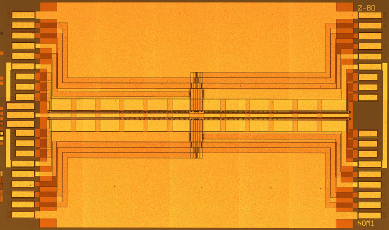
Thanks to Infineon Technologies, our industrial partner, we are allowed to design and produce complex 2D and 3D trap geometries with nanoscale precision and 100% reproducibility. For instance, we engineer structures to trap and move multiple ions, made of hundreds of electrodes addressed through vias distributed on multiple layers as in the figure below.

Scalable infrastructure
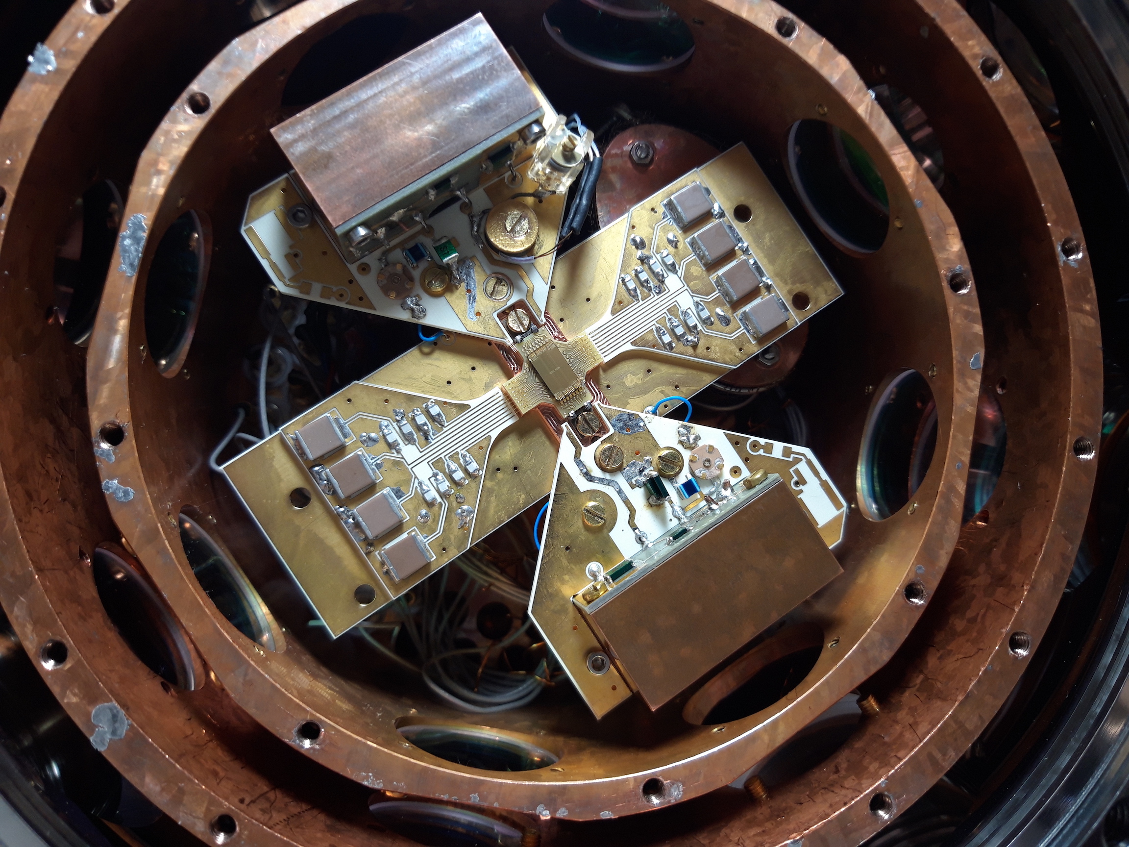
In order to trap, move [1] and make operations with many ions, we need an extremely stable environment. Our cryostat is a fast and reliable platform to test our ion traps since it provides extremely high vacuum and temperatures close to 4 K within few hours of operation. Low temperature minimizes the ion’s heating, and low pressure drastically diminishes the probability to observe collisions in between an ion and the background gas. On top of that, the cryogenic environment allows us to use semiconductor materials in the production of our traps.

Scalable fabrication
Silicon is a material of widespread use in electronics, for which a huge toolbox of fabrication techniques have been developed. This makes Si extremely appealable for quantum computing applications. Unfortunately, it has very high RF losses and we can mainly follow 3 approaches in order to build Si-based RF ion traps:
- highly doped (and thus conducting) Si is used instead of pure Si.
- a ground electrode is inserted between the silicon substrate and the trapping electrodes to shield the silicon from the RF fields.
- below 25 K, the charge carriers in intrinsic silicon freeze out, making the substrate a good insulator with low RF losses. This obviates the need for a shielding electrode, which in turn reduces the trap capacitance and the power dissipation, and allows us to harness new fabrication techniques.
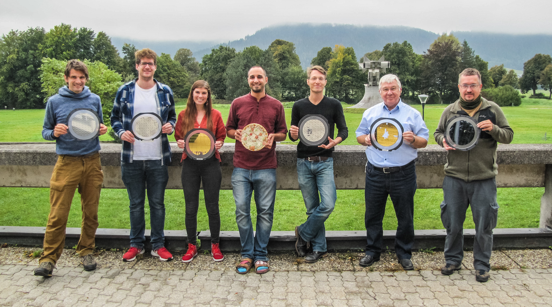
Project members

- Silke Auchter (PhD student)
- Marco Valentini (PhD student)
- Matthias Dietl (PhD student)
- Philip Holz (Postdoc)
- Thomas Monz (Senior Scientist)
- Philipp Schindler (Project leader)
- Rainer Blatt (Group leader)
Former members: Dominic Schärtl, Regina Lechner, Michael Niedermayr, Michael Brownnutt, Alexander Erhard (now with the LinTrap project), Davide Gandolfi, Adam Pauli, Gerald Stocker, Kirill Lakhmanskiy, Yves Colombe, Klemens Schüppert
References
[1] Philip C. Holz et al. “2D Linear Trap Array for Quantum Information Processing”. In: Advanced Quantum Technologies 3.11 (2020), p. 2000031. DOI
Recent publications
- “2D Linear Trap Array for Quantum Information Processing”, Philip C. Holz et al., Advanced Quantum Technologies 3.11 (2020), p. 2000031. DOI
- "Observation of superconductivity and surface noise using a single trapped ion as a field probe", K. Lakhmanskiy, P. C. Holz, D. Schärtl, B. Ames, R. Assouly, T. Monz, Y. Colombe, R. Blatt
Phys. Rev. A 99, 023405 (2019), arXiv:1805.00793 - "Electromagnetically-induced-transparency ground-state cooling of long ion strings", R. Lechner et al., Phys. Rev. A 93, 053401 (2016), arxiv:1603.05568
- "Operation of a planar-electrode ion-trap array with adjustable RF electrodes", M. Kumph et al., New J. Phys. 18, 023047 (2016), arXiv:1402.0791
- "Electric-field noise above a thin dielectric layer on metal electrodes", M. Kumph et al., New J. Phys. 18, 023020 (2016), arXiv:1511.00624
- "Ion-trap measurements of electric-field noise near surfaces", M. Brownnutt et al., Rev. Mod. Phys. 87, 1419 (2015), arXiv:1409.6572
- "Cryogenic surface ion trap based on intrinsic silicon", M. Niedermayr et al., New J. Phys. 16, 113068 (2014), arXiv:1403.5208
- "Compact radio-frequency resonator for cryogenic ion traps", D. Gandolfi et al., Rev. Sci. Instrum. 83, 084705 (2012), arXiv:1204.5004

